I am interested in this product
Close Form
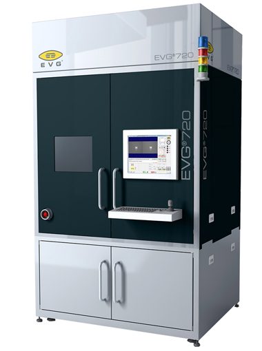
The EVG UV Nano Imprint Lithography supports hard and soft UV-NIL as well as micro-contact printing applications and includes dual-stage alignment approach for excellent overlay, a high-precision wafer stage and a unique imprint head allows for real time and in-situ characterization of embossing and de-embossing forces of various commercial available resists or anti sticking layers.
I am interested in this product
Close Form
Downloads
Detailed Specs
The EVG UV Nano Imprint Lithography series systems allows for imprint processes with stamps to substrates ranging from small chip size pieces up to 150 mm in diameter. Configurations for nanotechnology applications can include release mechanisms for stamps in addition to programmable high and low contact force. Uniform contact force for high yield large area printing is provided by EV Group’s proprietary chuck design which supports both soft and hard stamps.
The UV Nano Imprint Lithography system leverages EVG’s innovative SmartNIL technology and EVG’s materials expertise to enable mass manufacturing of micro- and nanoscale structures. Capable of printing nanostructures as small as 40 nm over a large area with unmatched throughput and low cost of ownership, the EVG system with SmartNIL technology is ideally suited for volume production of optics, photonics, light emitting diodes (LED), microfluidics and other bioMEMS devices, as well as advanced data storage. The UV Nano Imprint Lithography system supports hard and soft UV-NIL as well as micro-contact printing applications. Special system features include a dual-stage alignment approach for excellent overlay, a high-precision wafer stage and a unique imprint head which allows for real time and in-situ characterization of embossing and de-embossing forces of various commercial available resists or anti sticking layers. Additionally, a resist drop dispensing system for viscosities between 1 to several 1,000 mPas which improves the process flexibility for micro- and nano patterning. The UV Nano Imprint Lithography system is able to imprint in vacuum, which enables superior pattern fidelity, yield, and device performance. The system supports semi- and fullyautomated wafer and template transfer.