I am interested in this product
Close Form
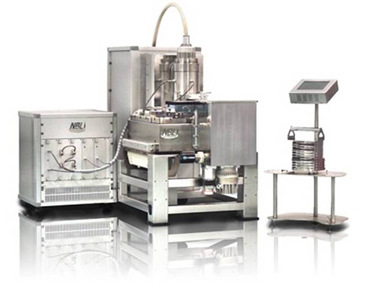
The nB5 electron beam lithography is a generation ahead of the current competition and with its field-proven performance has gained acceptance in the market place. It has excellent stability and has demonstrated an average uptime of greater than 93%.
I am interested in this product
Close Form
Downloads
Detailed Specs
Electron Beam Lithography (EBL) aims:
– Electron Beam Lithography’s refine design and components reduce routine service requirements.
– Achieve a machine-fault-downtime of less than 5% annually.
– Enhance performance.
– Facilitate volume production.
Specification:
– Maximum Substrate/ Wafer Size 200 mm Gaussain beam step and exposure writing statergy Beam Voltage range 20kV – 100kV Beam Currents from 0.1 nA up to 100nA
– Feature size on resist <8nm Laser interferometer stage with 0.31 nm resolution
– Stitching/overlay error <25nm for 500um field
– Automatic loading 5 chuck airlock system
– 20 bit DAC, 55 MHz pattern generator
– Full automated alignment
– 6 chuck substrate load lock
– Minimum Sopt Size < 5nm
The Electron Beam Lithogrpahy system will provide a platform for further development to high deflection speed and further integrated electronics.