I am interested in this product
Close Form
EV Group inspection systems are designed for highly accurate destruction-free alignment accuracy measurements and for all processes that involve double sided lithography. IR Inspection system are also used for wafer bond quality inspection
I am interested in this product
Close Form
Detailed Specs
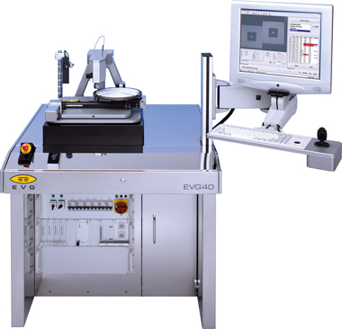
The EVG Semi-automated and the EVG Automated Measurement System/IR Inspection System performs highly accurate, non-destructive top-to-bottom side alignment accuracy measurement on double-sided structured wafers or bond interfaces as well as CD and Box-in-Box measurements of single and/or double side structured wafers. The Measurement/Inspection System can accurately measure any type of substrate material up to 200mm and 300 mm in size respectively. The measurement system is a highly flexible tool capable of measuring across the full wafer surface with an unlimited number of measurement points. With its flexibility it is suitable for different fields of applications like MEMS, sensors, micro-optics, power devices, compound semiconductors and silicon-based power devices, hybrid technology, multi-layers and all technologies that involve double-side lithography. For qualification of bond quality after pre-bonding, the IR Inspection System gives first information on the bond quality via a stored image. A uniform illumination system and an IR sensitive CCD camera are the main components of the IR-inspection station. Video frame grabbing technology displays the camera image on the process monitor. The image of each wafer can be optionally stored on hard disk drive as graphic file.