I am interested in this product
Close Form
Non Destructive Electrical Characterization using Terahertz Spectroscopy.
In just one single measurement, the system is able to provide precisely the following physical properties:
DC conductance, σDC
DC resistance, RDC
Carrier scattering time, t sc
Carrier density, Ns
Carrier mobility, μdrift
I am interested in this product
Close Form
Detailed Specs
ONYX GRAPHENE & 2D MATERIALS CHARACTERIZATION:
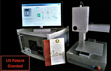
Onyx is the first system in the market designed to provide a full-area non-destructive characterization of Graphene, thin-films, and other 2D materials. Onyx covers the gap between the macro and the Nano scale tools characterizing from 0.5 mm2 to large areas (m2), enhancing the industrialization of the research materials.
Onyx is capable to measure the spatial distribution of the quality of the sample. Spatial resolution in the order of few hundreds of microns enable the fast characterization of large areas of sample as opposed to microscopic methods such as Raman, SEM, and TEM.
ONYX MOBILITY AND CARRIER DENSITY:
Onyx is continuously improving its features offering new results highly increasing its potential. Now, Onyx incorporates Mobility and Carrier Density analysis to its previous capabilities. In just one single measurement, the system is able to provide precisely the following physical properties:
• DC conductance, σDC
• DC resistance, RDC
• Carrier scattering time, tsc
• Carrier density, Ns
• Carrier mobility, μdrift
CAPABILITIES:
• Full Conductance/Resistance analysis
• Mobility and carrier density analysis
• Full sample inspection (100% area)
• Quality control of wide range of materials
• Non-destructive analysis
• No need for sample preparation
• Customizable inspection area (up to m²)
• Ultra-Fast –6 cm²/min
• Automated